

As RF systems become more compact and more complex, PCB designers face increasing demands to maximize the use of limited board area. High‑frequency architectures, such as phased arrays, MIMO systems, compact radar modules, and advanced sensing platforms, must support growing channel counts, improved isolation, and tighter performance margins while fitting into smaller footprints. Below are key reasons why space efficiency has become essential in modern RF PCB design: |  |
1. Increased Channel Counts Demand Smaller Footprints
Many next‑generation RF systems incorporate a much larger number of signal paths. Every added RF chain requires space for connectors, routing, isolation structures, and ground references. As channel density increases, connector footprint becomes one of the largest contributors to overall board size.
When component families occupy too much PCB real estate, designers may be forced to increase board dimensions, add extra layers, or sacrifice ideal placement, which increases cost or introduces performance tradeoffs.
2. Shorter Routing Paths Improve Signal Integrity
Space constraints directly affect routing length and structure. Longer RF trace runs:
- Raise insertion loss
- Increase phase variability
- Introduce additional parasitics
- Increase coupling risk
When layouts are tight, preserving short, direct routing paths becomes even more critical for maintaining predictable high‑frequency performance. Compact connectors and interfaces allow engineers to place the RF chain closer to the signal launch, reducing loss and ensuring consistent transition behavior.
3. Dense RF Architectures Require Strong Shielding and Grounding
As more RF channels are packed into a smaller area, maintaining isolation becomes harder. Designers must carefully manage:
- Consistent ground return paths
- Via fences
- Shielding shells
- Crosstalk mitigation strategies
In high‑density areas, even small layout misalignments can degrade isolation or generate unwanted radiation. Space efficiency must be implemented alongside strong electromagnetic control.
4. Mechanical Stress Intensifies as Layouts Shrink
Tighter layouts compress mechanical margins: connectors sit closer to edges, fasteners, or stacked modules. This can increase mechanical loads from vibration, thermal expansion, or frequent mating cycles.
Even in compact designs, connectors and interfaces must remain:
- Mechanically stable
- Resistant to vibration
- Durable under repeated servicing
- Easy to access for assembly
Shrinking the layout shouldn't compromise long‑term reliability.
5. Compact Designs Require Predictable Modeling and Integration
When space is tight, tolerances shrink. This increases the need for:
- Accurate 2D/3D models
- Reliable S‑parameters
- Verified pad and footprint geometry
- Recommended stack‑ups and layout guidelines
This reduces uncertainty and helps teams integrate high‑density features without extensive rework.
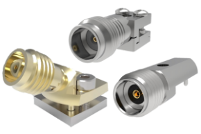
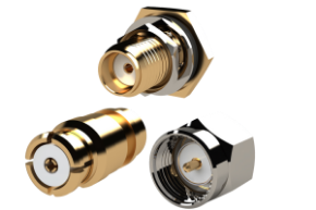
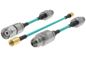
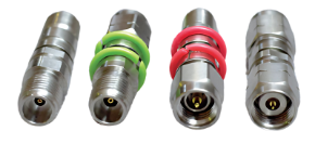
How the CoreHC™ Ganged RF Line of Products Supports These Challenges
After reviewing the major reasons space efficiency matters, it becomes clear how connector choices can influence the entire RF system architecture. CDI’s CoreHC™ Ganged RF Interconnect products were developed to address exactly these challenges across high‑density, high‑frequency PCB layouts. The CoreHC™ product family offers several advantages that align with the needs discussed above:
|
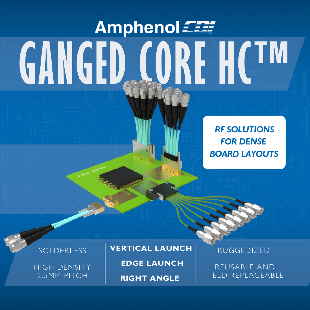
While no connector resolves every constraint associated with dense RF design, the CoreHC™ products provides a practical and well‑supported approach for engineers looking to optimize PCB area without sacrificing performance.